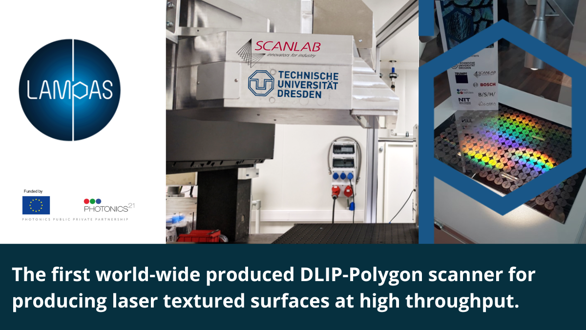
Press Release: LAMpAS announces the release of the first world-wide produced DLIP-Polygon scanner for producing laser textured surfaces at high throughput.
In the frame of the EU-funded LAMpAS project, the company SCANLAB and the Technische Universität Dresden have developed a high-speed speed polygon scanner unit, that is able to produce periodic surface patterns by utilizing the principle of interference. This device allows to produce patterns with feature sizes around 3.5 µm, which is about eight times smaller than using conventional polygon scanners operating with wavelengths in the infrared.
The polygon scanner system implements the Direct Laser Interference Patterning (DLIP) technology, which by combination of several laser beams allows to manipulate and control the intensity distribution of the laser energy which resolution up to the sub-micrometer range. In particular, combining two laser beams produced a line-like intensity distributions, where the lateral distance between the lines can be controlled by the intercepting angles between the beams.
“For producing patterns with short spatial distances, large intercepting angles are needed, which are impossible to reach using conventional polygon scanners. Furthermore, longer laser wavelengths require even larger angles compared to UV radiation. Therefore, we needed to develop a very special optical arrangement in order to obtain the needed angles,” says Ronny De Loor from SCANLAB.
“These small features are necessary since the functionalities of materials that we would like to improve can be enhanced in particular by reducing their size. This is in general what natural examples do,” added Prof. Andrés Lasagni from the TU Dresden and coordinator of LAMpAS project.
Since high throughput manufacturing also requires of high laser power, a unique special laser device has been also developed in LAMpAS project and is being combined now with the DLIP-Polygon head. “…It has been a challenging task to design an optical configuration capable to receive over 1 kW of optical power provided by pulsed laser source with pulse durations in the picosecond regime. This has not been done so far…”, explains Dr. Robert Baumann, also from the TU Dresden.
It is remarkable fact also that the final systems, which is being mounted in Belgium by LASEA, also includes two monitoring systems with independent techniques that are capable to assure the stability of the structuring process as well as the quality of the obtained surface properties. Thus, this innovative strategy aims to early detection of instabilities and malfunctions.
About LAMpAS
LAMpAS was set up in 2019 with a grant of €5.1 million under the EU’s Horizon 2020 program. The aim of this project is to develop the potential of laser structuring and to bring the technology to industrial levels at affordable costs. It aims at the design of newly functionalized surfaces by enhancing the efficiency, flexibility, and productivity of processes based on the development of a high-power ultra-short-pulsed laser system together with advanced optical concepts for high-throughput materials processing.
Inspired by nature, LAMpAS technology aims to produce well-defined periodic surface patterns with feature sizes smaller than 1 µm that can provide tailored surface functions for applications including anti-fingerprint, decorative, and easy to clean finishes for ovens, fridges, and other home appliances.
Details about LAMpAS can be found on their website https://www.lampas.eu/ and on their social media: https://www.linkedin.com/company/lampas-eu-project/ and https://twitter.com/lampaseuh2020
This project has received funding from the European Union’s Horizon 2020 research and innovation program under grant agreement No 825132. It is an initiative of the Photonics Public Private Partnership (www.photonics21.org).
The presented results reflect only the author’s view. The EU is not responsible for any use that may be made of the information it contains.

